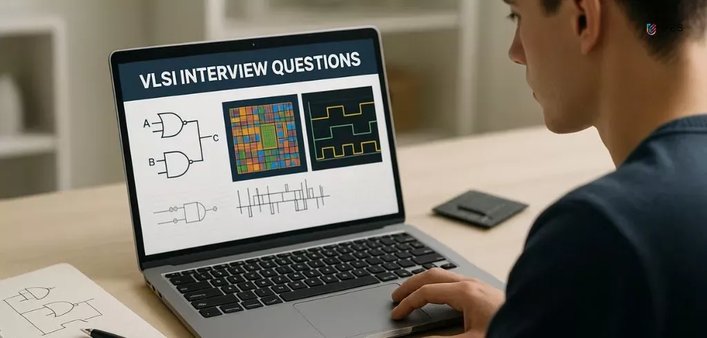
VLSI Interview Questions: Complete Q&A Guide for Students & Freshers
- UPES Editorial Team
- Published 09/12/2025
- VLSI Basic Interview Questions
- VLSI Interview Questions for Freshers (HR + Fundamentals)
- Digital Electronics Interview Questions for VLSI
- VLSI Technical Interview Questions (Timing, Power, Test)
- VLSI Physical Design Interview Questions
- Interview Questions for VLSI Engineer (Experience & Projects)
- Tricky VLSI Interview Questions (Conceptual Traps)
- FAQs on VLSI Interview Questions and Preparation
If you’re aiming for a chip-design or semiconductor job, you’ve probably already googled vlsi interview questions and landed on endless lists with no real explanations. That’s stressful and not very useful.
This guide is built differently. You’ll get carefully selected VLSI interview questions with full sample answers, grouped by topic. You’ll also see how a focused B.Tech in VLSI Design and Technology can help you actually understand these concepts instead of just memorising them.
Become future-ready with our Advanced Engineering programs
Know MoreVLSI Basic Interview Questions
Let’s start with core theory questions that almost every VLSI student faces.
Q1. What is VLSI?
- Answer: VLSI stands for Very Large Scale Integration. It refers to the process of integrating thousands to billions of transistors on a single chip to implement complex functions like processors, memories, and SoCs.
Earlier, circuits were built using discrete components. With VLSI, we pack logic, memory, I/O, and sometimes analog/RF blocks into a single IC, which reduces size, power, and cost, while increasing performance and reliability.
Q2. What is the difference between ASIC and FPGA?
Answer: An ASIC (Application Specific Integrated Circuit) is a custom-designed chip optimised for a particular application, such as a mobile SoC or network switch. It offers high performance and low power, but has high upfront cost (mask, design) and is not reprogrammable after fabrication.
An FPGA (Field Programmable Gate Array) is a reconfigurable device made of programmable logic blocks and routing. You can change its functionality after manufacturing using hardware description code. FPGAs are ideal for prototyping, low-volume products, and applications where flexibility is important, but they are usually larger, slower, and more power-hungry than ASICs for the same function.
Q3. What is the difference between synchronous and asynchronous circuits?
- Answer: In a synchronous circuit, all state elements (like flip-flops) are triggered by a global clock signal. This makes design, analysis, and verification easier because state transitions happen at defined clock edges.
In an asynchronous circuit, there is no global clock. Operations are driven by local handshakes and signal changes. Asynchronous designs can, in theory, be faster and more power-efficient, but they are harder to design and verify, so most commercial VLSI systems are predominantly synchronous.
VLSI Interview Questions for Freshers (HR + Fundamentals)
For vlsi interview questions for freshers, companies mix basics with HR-style questions.
Q4. Why do you want to work in VLSI instead of software?
Sample Answer: “I enjoy working close to the hardware and understanding how systems behave at the signal and transistor level. VLSI lets me combine my interest in electronics, maths, and problem-solving to design chips that become the core of devices people use every day.
While software is also attractive, I find it exciting that improvements in VLSI—like better power or performance—can impact millions of devices. I want to build a career in a field where my work contributes to that kind of deep optimisation.”
Q5. Which VLSI tools or languages have you used during your B.Tech?
Sample Answer: “During my B.Tech, I used Verilog/SystemVerilog for RTL design and simulation. For digital implementation and analysis, I’ve been exposed to tools like [mention typical tools you’ve used: e.g., Cadence/ Synopsys/Mentor equivalents used in your labs], and I’ve done basic synthesis and timing analysis exercises.
I’ve also worked with simulation tools for digital electronics labs and have some exposure to scripting in Python/Tcl for automation. I’m comfortable learning new EDA tools and workflows as required.”
Q6. Can you explain the difference between combinational and sequential logic with an example?
- Sample Answer: Combinational logic circuits produce outputs that depend only on the current inputs, with no memory. Examples include adders, multiplexers, and encoders- if the inputs change, the outputs change immediately based on the logic function. Sequential logic circuits, on the other hand, have memory; their outputs depend on both current inputs and past states. Flip-flops, counters, and registers are classic examples. In VLSI, we use combinational logic for data-path operations and sequential logic to store state, implement pipelines, and control timing across clock cycles.
Q7. Tell me about a VLSI or digital design project you’ve done and what you learned from it.
- Sample Answer: In my final-year vlsi project, I designed and verified a [say something generic if needed: e.g., ‘4-bit ALU / UART / simple RISC CPU core’] in Verilog. I started with a block-level specification, wrote the RTL, and then created a comprehensive testbench to cover different input scenarios and corner cases. Through this, I realised how important clean coding style, modular design, and proper reset/clock handling are. I also learned to debug timing and functional issues using simulation waveforms. The project gave me confidence that I can take a design from spec to RTL to verification in a structured way.
Q8. How do you plan to keep your VLSI knowledge updated over the next few years?
Sample Answer: VLSI is evolving quickly, so I know I can’t rely only on what I learned in college. I plan to regularly revise core concepts like CMOS, timing, and digital design, and then build on them through online courses, industry blogs, and documentation for the tools I use.
On the job, I want to learn from senior engineers by asking questions, reading their code and constraints, and understanding why certain design or implementation choices were made. I also intend to work on small side projects or experiments in Verilog/SystemVerilog to keep my hands-on skills sharp as I grow in the field.”
Quick Self-Check MCQ – Freshers
In a typical VLSI job role for freshers, which of the following matters MOST?
- Perfect English without any technical knowledge
- Deep VLSI fundamentals + ability to learn tools
- Knowing hundreds of EDA tools without basics
- Only having high CGPA
Correct answer: b) Deep VLSI fundamentals + ability to learn tools
Digital Electronics Interview Questions for VLSI
Digital fundamentals are the backbone of most vlsi interview questions.
Q9. What is setup time and hold time?
- Answer: For a flip-flop, setup time is the minimum time before the active clock edge during which the input data must remain stable. Hold time is the minimum time after the clock edge during which the data must remain stable.
If data changes within the setup or hold window, the flip-flop may go into metastability—an undefined state—leading to incorrect outputs or timing violations. In VLSI, we must ensure that all data paths satisfy both setup and hold constraints for correct operation at the target clock frequency.
Q10. What is a metastable state?
- Answer: A metastable state occurs when a flip-flop is unable to resolve its output to a definite ‘0’ or ‘1’ within the required time because the input changed too close to the clock edge (violating setup or hold time).
In practice, this appears as an intermediate voltage level or an unpredictable output. Metastability cannot be eliminated completely, but its probability can be reduced using techniques like synchroniser chains and careful clock domain crossing design.
Q11. Implement a 2:1 MUX using basic gates.
- Answer (conceptual):
A 2:1 multiplexer with inputs I0, I1, select S, and output Y can be implemented as:
[
Y = \overline{S} \cdot I0 + S \cdot I1
]
- This translates to:
- One NOT gate to generate S̅,
- Two AND gates (S̅ & I0, S & I1),
- One OR gate to combine both AND outputs.
VLSI Design Interview Questions (RTL & Logic Design)
Q12. What is the difference between combinational and sequential logic?
Answer: Combinational logic outputs depend only on current inputs—examples include adders, multiplexers, encoders, and decoders. There is no memory element.
Sequential logic outputs depend on current inputs and past history because they include memory elements like flip-flops and latches. Examples are counters, registers, and state machines.
In RTL design, you typically model combinational logic using continuous assignments or always_comb blocks, and sequential logic using edge-triggered always blocks.
Q13. What is RTL (Register Transfer Level)?
Answer: RTL is a level of abstraction where a digital system is described in terms of data transfers between registers and the operations performed on that data.
At RTL, you specify:
- Registers (storage elements)
- Combinational logic that computes next-state and outputs
- Clock and reset behaviour
HDLs like Verilog or VHDL are often used to write RTL code. Synthesis tools then convert RTL into a gate-level netlist.
Q14. What is the difference between blocking and non-blocking assignments in Verilog?
- Answer: In Verilog:
- Blocking assignment (=) executes in order, like normal C statements. The next statement executes only after the current one finishes. It is generally used in combinational always blocks.
- Non-blocking assignment (<=) schedules all right-hand side evaluations first and updates the left-hand side at the end of the time step, making all assignments appear to happen in parallel. It is used in sequential (clocked) always blocks.
- Blocking assignment (=) executes in order, like normal C statements. The next statement executes only after the current one finishes. It is generally used in combinational always blocks.
Using them incorrectly can cause mismatches between simulation and synthesis or unintended latches and race conditions.
Salary Insights: How much does a VLSI Engineer Earn?
VLSI Technical Interview Questions (Timing, Power, Test)
Q15. What is clock skew and how does it affect timing?
Answer: Clock skew is the difference in arrival time of the clock edge at different flip-flops in the design. Ideally, all flip-flops receive the clock simultaneously, but in reality, routing delays and clock tree differences cause skew.
- Positive skew (destination clock arrives later) can help setup time but can hurt hold time.
- Negative skew (destination clock arrives earlier) can hurt setup time.
- Clock skew is managed through careful clock tree synthesis (CTS) and timing analysis to ensure that setup and hold constraints are still met.
Q16. What is the difference between static and dynamic power in VLSI?
- Answer: Dynamic power is consumed when transistors switch states—charging and discharging capacitors. It mainly depends on switching activity, capacitance, supply voltage, and frequency:
[
P_{dynamic} \approx \alpha C V^2 f
]
- Static power is consumed even when the circuit is not switching, due to leakage currents in transistors (subthreshold leakage, gate leakage, etc.). At deep submicron nodes, static power has become a major concern.
- Low-power design techniques target both: clock gating, voltage scaling, and activity reduction for dynamic power, and multi-Vt cells, power gating, and careful device choices for static power.
Q17. What is DFT (Design for Testability)?
- Answer: DFT refers to adding extra structures and design techniques to make a chip easier to test after fabrication. Because direct access to internal nodes is limited, we insert features like scan chains, built-in self-test (BIST), boundary scan, etc. These allow test equipment to:
- Control internal flip-flops as if they were primary inputs
- Observe internal states as if they were primary outputs
- Effective DFT improves test coverage and reduces the cost and time of production testing.
VLSI Physical Design Interview Questions
Physical design is a major area for vlsi interview questions, especially in backend roles.
Q18. What are the main steps in the VLSI physical design flow?
Answer: Typical physical design flow includes:
- Floorplanning- Deciding the placement of major blocks, I/Os, and power grid.
- Placement- Placing standard cells within the floorplan.
- Clock Tree Synthesis (CTS)- Building the clock distribution network.
- Routing- Connecting all nets using available metal layers.
- Optimisation- Fixing timing, power, and congestion issues (ECOs, buffering).
- Signoff- Final checks: STA, IR drop, EM, DRC, LVS before tape-out.
Each stage feeds into the next, and timing closure often requires multiple iterations.
Q19. What is congestion in physical design and how do you reduce it?
Answer: Congestion occurs when too many nets try to pass through a small physical area, and there are not enough routing resources. This can lead to routing failures, detours, and timing problems.
To reduce congestion, designers may:
- Improve floorplan (better macro placement, adding channels)
- Use cell spreading or density control
- Move or re-orient macros
- Use more metal layers or change routing constraints
- Perform timing and placement-driven optimisation
Q20. What are DRC and LVS?
Answer: DRC (Design Rule Check) verifies that the layout follows all foundry-specified geometric rules (minimum width, spacing, enclosure, etc.). Violations can make the chip non-manufacturable.
LVS (Layout Versus Schematic) checks that the layout connectivity matches the original schematic/netlist. It ensures that no devices are missing or connected incorrectly.
Both are critical signoff checks before tape-out.
Interview Questions for VLSI Engineer (Experience & Projects)
Once you have projects or internships, interview questions for VLSI engineer become more project-focused.
Q21. Explain a VLSI-related project you have worked on.
Sample Answer: In my final year, I worked on designing and verifying a 32-bit pipelined RISC processor in Verilog. The goal was to implement a simple instruction set with stages like fetch, decode, execute, memory, and write-back.
I was responsible for writing the RTL for the ALU and control unit, as well as creating a SystemVerilog testbench that checked instruction execution against expected results. We verified the design using multiple test programs and analysed timing after synthesis. This project gave me hands-on experience with RTL design, basic pipelining concepts, and verification.
Q22. How do you debug a timing violation reported by STA?
Sample Answer: First, I look at the timing report to identify whether it’s a setup or hold violation and note the worst violating path. Then I examine the path’s start and end points, intermediate cells, and logic depth.
For setup violations, I may try cell upsizing, buffer insertion, or logic restructuring to speed up the data path, or reduce clock frequency if possible. For hold violations, I might add delay buffers in the data path. After each change, I rerun STA to ensure that fixing one violation does not create new ones elsewhere.
Tricky VLSI Interview Questions (Conceptual Traps)
Some tricky vlsi interview questions are concept-based and test whether you really understand, not just memorise.
Q23. Can you remove hold time violations by reducing the clock frequency?
Answer: No. Hold time violations are independent of clock frequency. They depend on data arriving too early after the clock edge at the destination flip-flop. Reducing clock frequency increases clock period, which helps with setup violations, not hold violations.
To fix hold violations, you need to add delay in the data path or adjust clock skew, not change the clock period.
Q24. If a design has no setup violations at typical corner, is timing closure guaranteed?
Answer: No. Passing at a single typical corner is not enough. Timing closure must be verified across multiple corners and modes:
- Different process corners (SS, TT, FF)
- Different voltages and temperatures
- Different operating modes (functional, scan, etc.)
Setup and hold behaviour can change across corners, so closure must be done multi-corner, multi-mode (MCMM).
Short Trick Question
Which of these reduces dynamic power the most (all else equal)?
- Increasing supply voltage
- Decreasing switching activity
- Increasing frequency
- Increasing load capacitance
Correct answer: 2) Decreasing switching activity
How a Focused B.Tech in VLSI Design & Technology Helps
To handle these vlsi interview questions confidently, you need more than last-minute notes. You need:
- Strong fundamentals in digital electronics, devices, and circuits
- Exposure to HDLs (Verilog/SystemVerilog) and simulation
- Understanding of backend concepts like floorplanning, CTS, routing, and STA
- Practice with industry-relevant tools and flows
A specialised programme like B.Tech in VLSI Design and Technology at School of Advanced Engineering UPES is designed to build exactly this skill set.
- A curriculum focused on semiconductor devices, digital design, VLSI design, and physical design
- Labs and projects using industry-style EDA tools
- Opportunities for internships, industry projects, and expert lectures
- Placement support for roles like VLSI design engineer, verification engineer, physical design engineer, DFT engineer, etc.
If you’re serious about building a career in chip design and want structured preparation for future VLSI interview questions, explore the B.Tech VLSI Design and Technology programme here.
FAQs on VLSI Interview Questions and Preparation
1. What topics should I focus on most for VLSI interviews as a fresher?
Focus on digital electronics, CMOS basics, HDL (Verilog/VHDL), basic VLSI design flow, timing (setup/hold), and simple physical design concepts. You don’t need to know everything deeply, but your fundamentals must be very clear.
2. Are VLSI interview questions very different for design and verification roles?
- The fundamentals are similar, but design roles focus more on RTL, architecture, and synthesis, while verification roles emphasise testbenches, coverage, assertions, and methodologies like UVM. Both expect strong digital fundamentals and basic VLSI knowledge.
3. How important is tool knowledge for a VLSI fresher?
- Companies don’t expect you to master every EDA tool, but they like to see comfort with at least one flow (e.g., simulation + synthesis) and a willingness to learn. Fundamentals matter more; tools can be taught on the job.
4. Do I need a specialised VLSI degree, or is general ECE enough?
- Many VLSI engineers come from ECE backgrounds, but a specialised VLSI programme can give you more focused exposure to design/physical flows, tools, and projects, which helps in interviews and early career growth.
5. How should I practise for VLSI interviews?
- Revise theory, solve numericals, and actively explain concepts aloud as if teaching someone. Work through small RTL or digital design examples, and, if possible, implement and simulate them. Use actual interview-style vlsi interview questions like the ones in this blog as mock practice and read books on VSLI Technology.

Our counsellors are just a click away.
Conclusion
Instead of collecting dozens of random PDFs, use a structured set of vlsi interview questions like this to guide your preparation. Make sure you can:
- Explain each concept in your own words
- Draw simple diagrams or timing waveforms where needed
- Connect answers back to real projects or lab work you’ve done
If you’re still at the stage of choosing your degree or specialisation, and you know you want to be in chip design, then investing in a focused B.Tech in VLSI Design & Technology can give you the right foundation and industry exposure to make interviews far less scary.
UPES Editorial Team
Written by the UPES Editorial Team
UPES Admission Enquiry
Subscribe to UPES Blogs
Join our community for exclusive stories, insights, and updates
By clicking the "Subscribe" button, I agree and accept the privacy policy of UPES.


